News – archive
X-ray Diffraction
CHANL is thrilled to offer powder and thin film x-ray diffraction with a new Rigaku SmartLab x-ray diffractometer (XRD). This system is capable of grazing angle measurements for measuring diffraction from thin films, and an in-plane diffraction arm for measuring crystalline planes perpendicular to the sample surface. Samples with periodicity on length scales up to 100 nm can be characterized with the SAXS unit, and micro area measurements with spot sizes as small as 100 um are also possible. Rocking curves, pole figures, and reflectivity measurements are all available with this system, which is also equipped with a HyPix-3000 2D detector. A number of sample stages allowing for sample heating and cooling (-100ºC to 1,000ºC) and environmental control (inert atmosphere, vacuum, reactive gas) are available for interesting in-situ measurements. The SmartLab Guidance software makes these measurements easy to implement as it guides users to install the correct optical components, and walks them through the appropriate alignments before measurements begin. Powerful analysis software includes access to the ICDD PDF2 database, allows for Rietveld whole pattern fitting, and 2D pattern analysis.
For more information on the instruments specifications or if you would like to be trained to use these systems, please contact Carrie Donley.
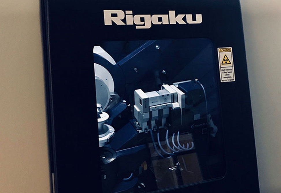
Rigaku SmartLab X-ray Diffraction
Infrared Spectroscopy
The Hyperion 1000 with Tensor 27 by Bruker Optics is an FTIR microscope allowing for microanalysis in transmission, reflection, or ATR mode. In addition, a standard Tensor spectrometer allows for traditional FTIR measurements as well. The system has recently been upgraded with a new MCT detector, a motorized stage for the microscope, polarizers, a variable angle ATR accessory, and new software.
For more information on the instruments specifications or if you would like to be trained to use these systems, please contact Carrie Donley.
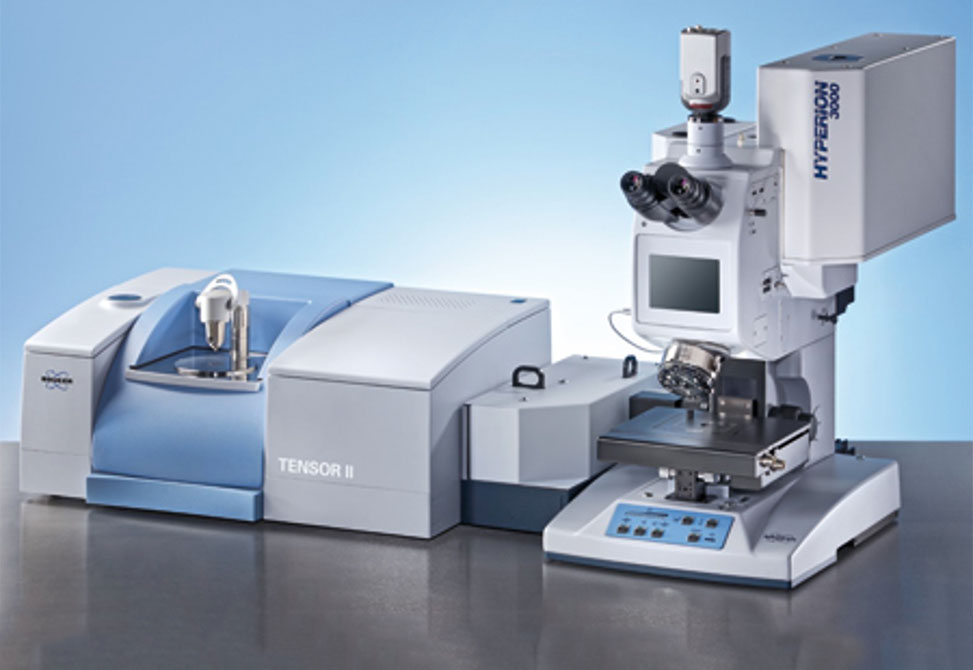
Hyperion 1000 with Tensor 27
E-beam Evaporation
CHANL has installed a new PRO-Line PVD 75 E-beam evaporation system in the cleanroom. Capabilities of the system includes:
- Load-locked tool can reach 10-8 Torr range in minutes
- High vacuum chamber reduces surface oxidation
- Line-of-sight deposition for lift-off and shadow masking techniques
- Automated deposition rate and endpoint control
- Water cooled substrate holder
For more information on the instruments specifications or if you would like to be trained to use these systems, please contact Jun Yan.
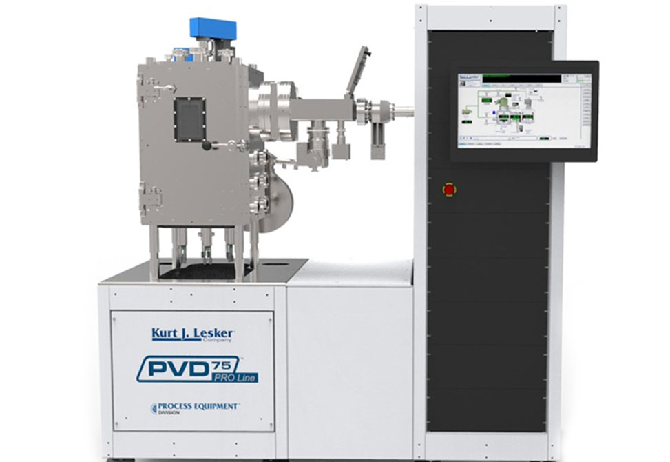
PRO-Line PVD 75 by Kurt J. Lesker Co.
E-Beam Lithography
CHANL has installed a new Nanometer Pattern Generation System, NPGS, on our focused ion beam system. The NPGS is designed as an e-beam lithography system, but can also be used with the focused ion beam too. The system can achieve patterning with resolution on the order of less than 20nm for the electron beam and less than 50nm for the ion beam. If you need to pattern features that are smaller than what we can do with photolithography, ~1 um, this system may be able to help you.
For more information on the instrument specifications or if you would like to be trained to use this system, please contact Jun Yan
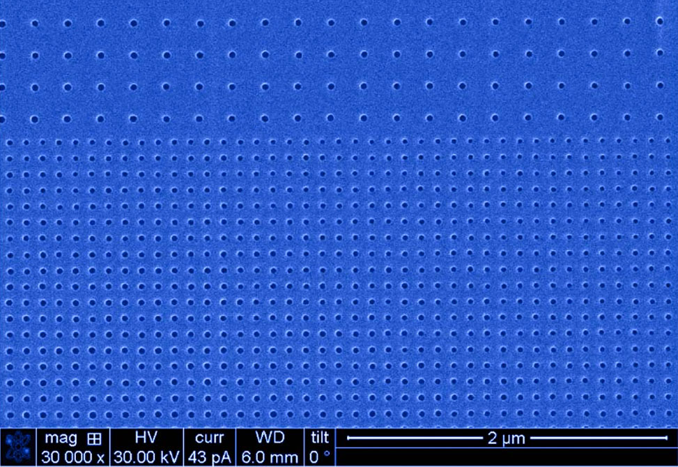
E-beam written dots less than 20nm in silicon wafer
Atomic Layer Deposition
Although CHANL already had one ALD system, we have added a new system to our inventory. The first one was heavily booked and there were limited precursor lines, which limited our ability to try out new precursors while keeping the original tool available for routine work.
The new ALD system has allowed us to add 6 precursor lines, including a low vapor pressure, VLP, delivery line, and has also relieved some of the scheduling pressure that users were experiencing on the original system. New precursors that we have been exploring since the purchase of the new system include a number of metal organics for depositing CuO, Ga2O3, HfO2, Nb2O5, WO3, and ZnO.
For more information on the instruments specifications or if you would like to be trained to use these systems, please contact Bob Geil.
Voltage Contrast
Voltage contrast is a new mode of imaging recently explored in CHANL for the FIB, FEI Helios, and ESEM, FEI Quanta. Voltage contrast allows users to clearly differentiate electrically connected components from disconnected components. Contrast occurs when the incident beam charges the floating/disconnected region on the sample causing it to appear brighter when imaged with the electron beam or darker when imaged with the ion beam.
The regions of the sample that are electrically connected to the SEM ground are able to dissipate any charging and appear dark when imaged with the electron beam or bright when imaged with the ion beam. Contrast can be amplified by applying an external bias to the connected region, a process commonly referred to as active voltage contrast. The simplicity of the process is ideal for quickly and precisely identifying failures in nanoscale electronic devices/integrated circuits, determining network connectivity in percolation networks, finding disconnected regions in thin films, and a variety of other applications.
If you are interested in trying this out on your samples, please contact Wallace Ambrose.
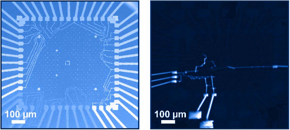
Example of negative, left, and positive, right, voltage contrast resulting from charging with the electron beam and ion beam for two distinct circuits. On each circuit a bottom metal pad is connected to the SEM ground through a wire bond off screen.
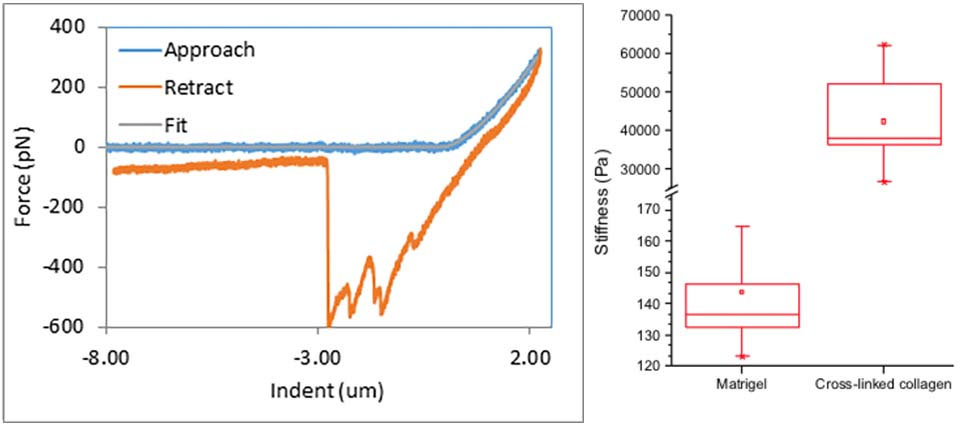
Elastic Modulus Measurements on Soft/Sticky Materials in Fluid
CHANL has worked to develop and document methods to measure the elastic modulus of materials with AFM force measurements. Researchers in the biomedical engineering focused Allbritton Lab, were interested in understanding how the stiffness of their matrix affected cell growth. These samples were soft and sticky and needed to be measured in fluid so that they would stay hydrated.
Using large colloid probe tips, CHANL researchers, relying on advice from researchers in the Superfine Lab, physics, were able to extract elastic modulus values from these samples. A representative force curve showing the approach, blue, and retract, orange, for a Matrigel sample is shown in the figure to the right.
The large negative forces indicate the adhesion forces between the tip and the sample surface before the tip finally pulls out of the sample. A comparison of stiffness values of a soft extracellular matrix, Matrigel, and fully chemically cross-linked calf-skin collagen surface, is shown on the far right, and other samples are also under investigation. Data was acquired by Nicole Smiddy with the Allbritton Lab.
If you have questions about this technique or would like to make similar measurements on your samples, contact Carrie Donley.
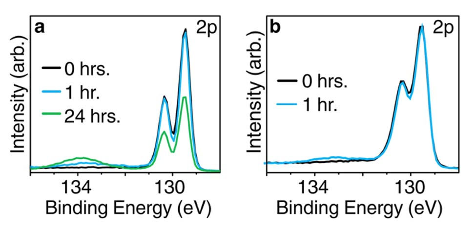
Air Sensitive XPS/UPS Measurements
Researchers in Scott Warren’s lab in Applied Physical Science & Chemistry, were interested in studying phosphorene, atomically thin layers of phosphorus, but this material is extremely air sensitive, and is typically handled in a nitrogen purged glovebox. Quantitating the rate of oxidation for this material was going to be difficult, but CHANL was able to design a system to help.
Carefully controlled introduction of samples into the XPS chamber prevented oxidation of these samples, and also allowed for controlled studies of the oxidation rate. The P 2p data below shows the elemental phosphorus doublet around 130 eV, and the growth of the oxidized product around 134 eV with air exposure for (a) bulk and (b) few layer black phosphorus. This sample loading technique has also been successfully applied to air sensitive samples from other research groups as well.
If you are investigating air sensitive samples with XPS or UPS, contact Carrie Donley (cdonley@email.unc.edu) for more information.
If you have questions about this technique or would like to make similar measurements on your samples, contact Carrie Donley.
Woomer, A.H.; Farnsworth, T.W.; Hu, J; Wells, R.A.; Donley, C.L.; Warren, S.C. “Phosphorene: Synthesis, Scale-Up, and Quantitative Optical Spectroscopy” ACS Nano 2015, 9, 8869-8884.